Printed Circuit Boards
In the good old days, circuit board layout was a tedious exercise. You had to lay all the pads out (the places where the legs of the electronic components go through the board) by hand. The tracks were also placed by hand, using transparent strips. For a double-sided board, you would use two different colours, one for each side, normally red and blue. This told the PCB manufacturer which side you wanted the each set of tracks. These were stuck down on a transparent polyester base. This was normally done at twice the size, so that when it was scaled down to the actual PCB size, it would be more accurate.
Since then, as with so many things, computers have made life a whole lot easier. Many PCB design programs available now have routing checkers that test for potential errors. I couldn't quite run to that, so I got a relatively cheap solution.
These days, the majority of circuit boards use Surface Mount Technology (SMT). This means there are no component legs that go through the board. SMT boards are normally made "out of house" (somewhere like China), as the facilities needed, and labour costs for assembly weigh heavily! SMT can make boards very densely packed, therefore very compact in size. Modern PCB's can be horrendously complex, and be consisted of multiple layers (up to 24 or so).
The PCB's for this project however, are just double-sided, component-through-hole designs.
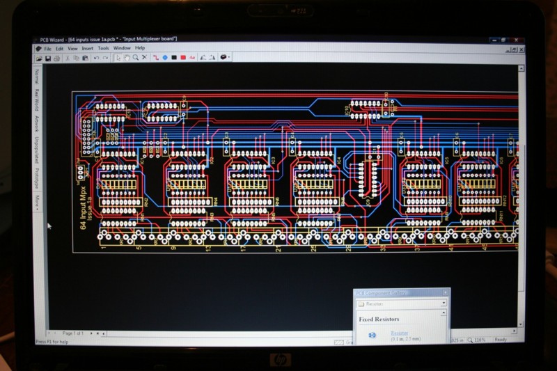
Below is a screen shot of the input board from the PCB design program. This wasn't during the actual development phase (I've just taken this screen-shot from my laptop). All the shots after this however were taken during, or just after the actual board design period.
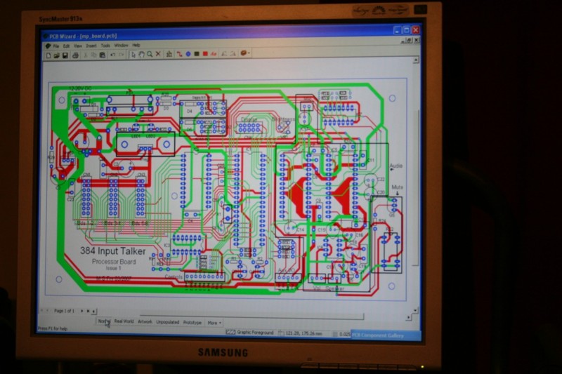
Below is a screen shot of the processor board.
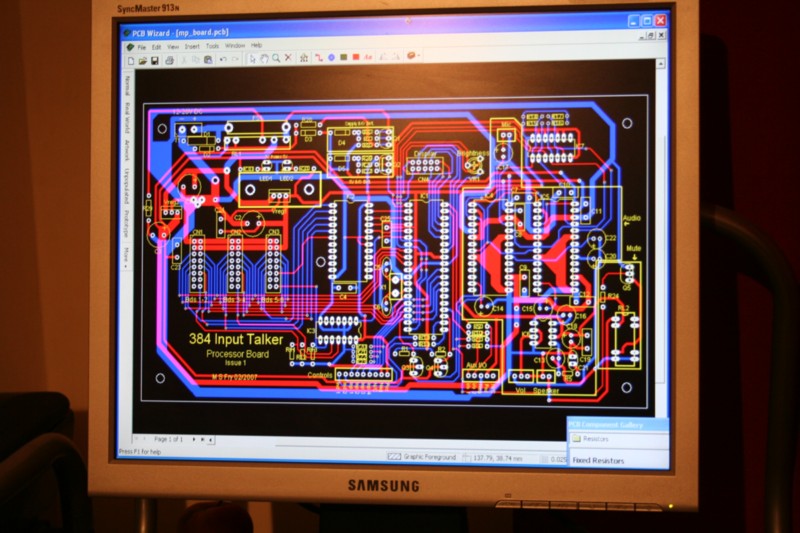
Below is a similar shot to the one above, but in the classic colours.
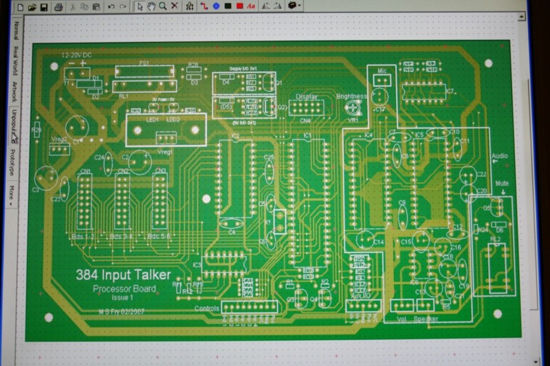
Finally, as I don't have a photo of the unpopulated processor board to hand, here is a visulisation of it in the PCB design program.